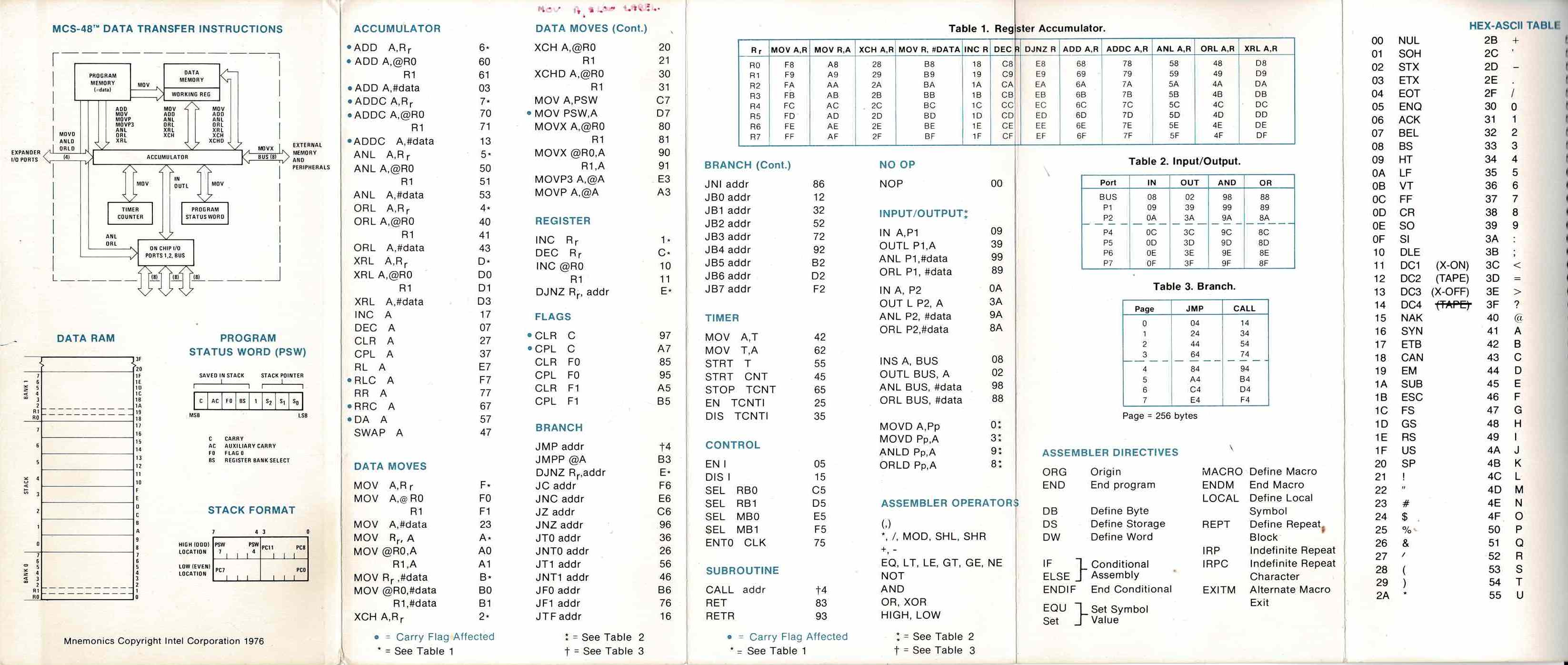
For those who have only worked with computers built with von Neumann or Princeton architecture, i.e. where both data and instructions are located in a common memory, the architecture of Intel’s 8048/8049 (called MCS-48) and later 8051 (called MCS-51) may seem somewhat alien. Data and program are separated and have separate address ranges. This is also known as Harvard architecture.
The program memory in an 8048 consists of 1K bytes, addressed in hexadecimal from 000H to 3FFH. In an 8049 there are 2K bytes addressed from 000H to 7FFH. Each of these processors can also address 2K of external memory, which will be located in addresses 800H to FFFH. In an 8048 this leaves a gap of 1K, from 400H to 7FFH. Addressing is limited to a 12-bit value, so 4K is the maximum that can be addressed. The program memory is divided into pages of 256 bytes each. The destination for a conditional branch instruction can only be within the same page that the instruction is located in. In addition, the program memory is divided into two memory banks, each with 8 pages or 2K memory. There is an unconditional jump instruction and an unconditional call instruction that can jump to any 11-bit-long address within a particular memory bank, which can be selected in advance with a memory bank select instruction. A call instruction stores a 12-bit return address in the stack.
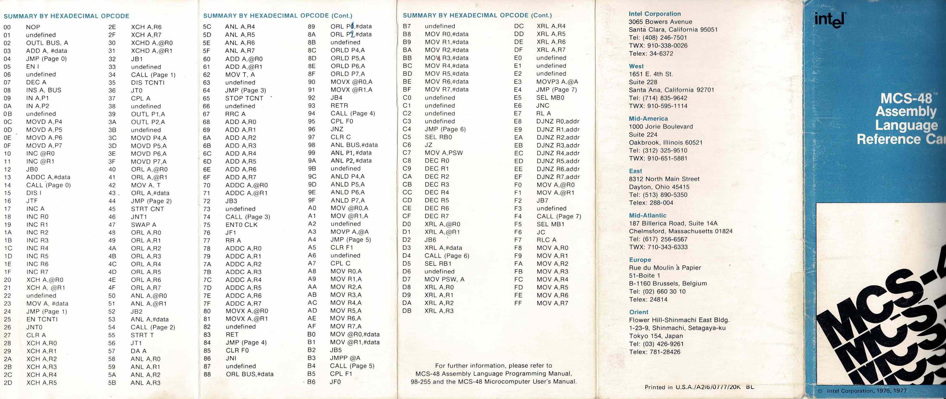
Each instruction consists of one or two bytes.
The data memory is addressed from 00H to FFH, i.e. a maximum of 256 bytes of internal data memory. In addition, up to 256 bytes of external data memory can be addressed, also with address range from 00H to FFH. Different instructions are used to fetch and store external data memory.
The internal data memory is divided into 8 registers (R0 to R7) in register bank 0 from address 00H to 07H, 16 bytes stack (8 levels) from 08H to 17H, and 8 registers in register bank 1 from address 18H to 1FH. The memory from 20H to FFH (20H to 7FH in 8048) can be used freely. There are instructions for register bank selection, typically done in interrupt routines to avoid having to store the registers used by the interrupt routine. The stack stores two bytes for each subroutine call or interrupt. There are 12 bits for the return address and 4 bits for status.
Input and output also have a special set of instructions for reading from and writing to the external ports and pins.
All calculations and all movement of data is done via an accumulator, A. However, it is possible to increment and decrement a register or increment an indirectly addressed byte in data memory. There are no instructions for moving data between registers.
Intel’s assembler was a macro assembler, so I had defined a set of macros that were passed from one project to the next. For example, there was a macro to add the contents of register R1 to a two-byte BCD (Binary Coded Decimal) value in RAM, which required 10 machine instructions.
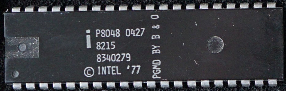
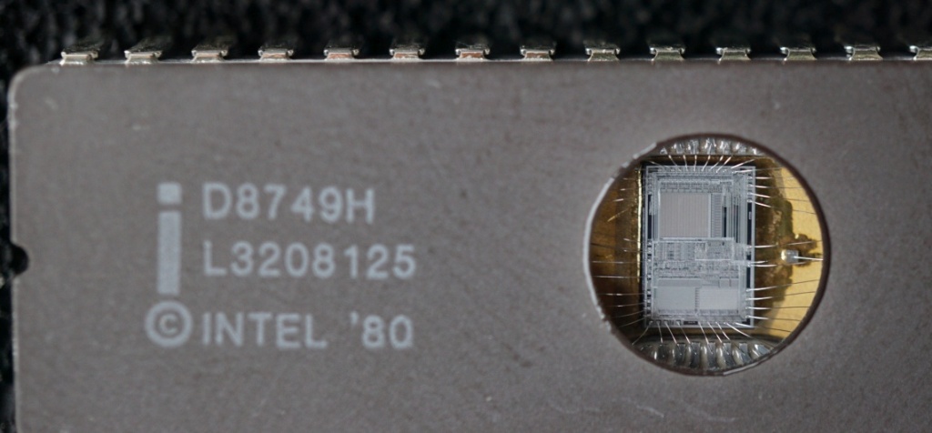
One of the advantages of the Intel processors was that they were available in an EPROM version, i.e. with a program memory that could be erased with ultraviolet light and rewritten, which was fully compatible with the final mask-programmed versions. These were called 8748 and 8749. The Intel 8748 was available when the processor was first used, but the 8749 came after the first project which used it. A small circuit board with an 8039 processor (an 8049 without data memory) and an external EPROM and I/O expander could be plugged into the 8049 socket and used to emulate an 8749.
Next chapter: Literature
