The distribution and use of I/O (input/output) pins on the processor was often a problem that required close cooperation between the programmer and the electronics developer on a project. There were a number of issues to consider, depending on the architecture of the processor, the wiring requirements, and the external components that would be controlled by or provide signals to the processor.
From 1976 to 1984, NMOS (n-type metal-oxide-semiconductor) was the most widely used technology for microprocessors. This technology uses a +5V power supply, and for digital logic there are levels for a signal to be considered low (typically < 0.8V) or high (typically > 2.0V). Input between these two levels is undefined, and can be seen as either low or high (digital 0 or 1). An earlier technology, PMOS (p-type metal-oxide-semiconductor), was still used for some processors, e.g. the TMS1000 from Texas Instruments which was used for the Beocenter 7700 terminal, among others. These used a negative power supply, and were not directly compatible with NMOS components. Around the mid-1980s, CMOS (complementary metal-oxide-semiconductor) became the most widely used technology, not least because of its lower power consumption, typically with a 3.3V power supply for the processor.
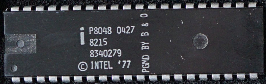
Some I/O pins can only be used for special purposes, some can only be used as input, some only as output, and others can be optionally set or switched between input and output. For example, the Intel 8048/8049 has an external interrupt pin, /INT, that can be used to provide an interrupt when it externally switches from a high level to a low level, or the value can be tested with a JNI instruction; a T0 pin whose input level can be tested directly with JT0 and JNT0 instructions; a T1 input pin which can either be tested with JT1 and JNT1 or used as an event counter (counting the number of high to low edges on the T1 input pin); port 1 and port 2 with 8 input/output pins each; and BUS (or port 0) which can be used either as 8 output pins or as 8 input pins, or as a true two-way port with strobe. However, with an external memory chip connected, BUS and part of port 2 are reserved for communication with the external chip and therefore cannot be used as regular I/O pins.

On some processors there are configuration registers which are used to set I/O pins as either input or as output. Other processors instead set an input pin to a high value and have an internal pull-up resistor, which can then be pulled low by an external signal and read as input.
If the processor, together with any external expander circuit, does not have enough I/O pins, there are various options for expanding the number of I/O pins. Among the options used in various devices are:
1. using the same I/O pins for different purposes, e.g. a strobe used for selecting a row on the keyboard can be used at the same time for selecting digits in a display. The keys were distributed in a matrix format of a number of rows and a number of columns, e.g. 6 rows and 5 columns in the Beocenter 7700. For key input one of the 6 rows is set low (called a strobe) and after a short pause the 5 column inputs are read. The strobe for the keypad is simultaneously used to select a digit in the display. Similarly, two latch circuits (a circuit holding output values) can be shared on some data output pins, with a separate chip select output to select between these two circuits.
2. If only one of a number of related pins is to be set at any given time, a 3 to 8 external expansion chip can be used. A value from 0 to 7 is set on the 3 output pins of the processor, and the external circuit sets the corresponding one out of eight output pins. This can be used, for example, to select a row on a keyboard with up to 8 rows of keys. In the Beocenter 7700, 3 output pins are used to select one of six strobes for the keyboard and display. Output number 7 from the expansion circuit is used as a chip select for a latch circuit which stores LED output values.
3. An external serial switch register can be used. Thus, on the microprocessor, an output pin for clock and one for data, and possibly one to control latching of the output in the external circuit are used. This is used for example in the Beocenter 7700 terminal for LCD display output.
4. A microprocessor with I2C bus can be used, or an I2C bus can be simulated in a processor where the bus is not built-in. There are a number of circuits that can be directly connected to this bus to provide input or control output. A simulated I2C bus was used in at least one of the Philips video recorders converted to B&O video remote control, and an I2C bus was built into the Philips 8400 processor used in the 37XX TV.
In most programs I wrote, the timer interrupt routine was used for all input and output. This was done partly to ensure that the time could be controlled reasonably accurately. This was especially important with time critical signals such as remote control and data link, and strobes for display and keyboard. A strobe for the keypad could be set in a timer interrupt and the key input read in a subsequent pass before the next strobe was read out.
There were some considerations to be taken when there was a mix of input and output on the same port. On processors like the Intel 8048/8049, on an 8-bit port you can only write all 8 outputs simultaneously. It is not possible to write a single output pin without all the other pins being written as well. The easiest solution was to use a byte in RAM to hold the values to be written to the port. You could then use an OR instruction to set a single bit, AND to clear a single bit, or XOR to invert a bit without changing any of the other bit values.
Other processors had the I/O ports addressed as fixed addresses in ordinary RAM. Here you could use AND, OR and XOR instructions directly. However, this could cause problems, as these obviously read the port to find the previous value before the new value was written. An input port could then accidentally be changed from input to output if the input value was 0, or an output port that was supposed to be high but was pulled low externally could be written with an incorrect output value. So again it was an advantage to have an image of the port stored in RAM.
For output ports, the processor uses active circuits to make the switch from low to high or from high to low. After a fast switch to high, the level is held with an internal pull-up resistor, typically around 50 kΩ, which can only supply a small current. The fast changess result in electromagnetic noise radiation which can cause problems if not shielded or dampened, as was first experienced when the Beocenter 7000 was in test production.
As Egon Bjerre, who was responsible for electronics in the Beocenter 7000, remembers:
During the development of the Beocenter 7000, I came into contact with a microprocessor for the first time. A lot of functions were controlled from here, so the design was very different from what we had done before.
Something new was also that there was now an oscillator on board. It was at 5.185 MHz. During development, EPROMs were used and this did not cause any problems.
As we approached the start of production, we switched to mask-programmed processors, and everything seemed to work well. That is, until one employee wondered about a howling sound when listening to P2, which was then at 98.5 MHz. It turned out to be the 19th harmonic from the oscillator, which hit that frequency and produced a very annoying interference.
It turned out that several of the microprocessor’s pins were sources of the interference, and the connected wiring was an effective antenna for the interference. It was clear that the best solution would be to place the microprocessor in a metal shield box, but we were close to the start of production and introducing a shield box would cause significant delays.
The solution was shielding on both sides of the processor. Next, resistors were inserted on many of the pins, along with decoupling capacitors.
The wiring for the FM antenna signal was made more “insulated” inside the device so that it was less sensitive to interference.
The solution was eventually acceptable, but we learned that microprocessors belong in a metal shield box.
Next chapter: Intel 8048/8049 architecture

This comment was originally submitted on the Danish-language version of this chapter by Tom Jelsing. Translated to English with the help of DeepL.com.
Thoughts about input/output
Hi Arne
I think it is a good description you have made of the microprocessor inut/output. Maybe you could also write a bit about how we saved I/O ports by multiplexing keyboard input and display output into a matrix.
At B&O we were actually one of the first in DK to develop products that contained both sensitive analogue electronics and digital electronics. I had a pretty good feel for the activities in this area at the time, as I was on the board of SMT (Society for Microprocessor Technology) for several years. The association was run by Elektronikcentralen (EC) and among the other members was e.g. Søren T. Lyngsøe, Radiometer, Brüel&Kjær, Storno, Phillips and several others whose names I have forgotten. The association financed a large number of studies and investigations, which were documented in relevant reports. I have saved a few of those that covered my area of interest: ECR 199 – Human Machine Interaction, ECR-226 – Design of Front Panels and Data Screens and ECR 227 – Usability in Practice.
Other topics that were very hot at the time were testing of microprocessor/memory ICs and EMC (Electro Magnetic Compatibility). As far as testing of electronic components was concerned, EC had the expertise and the necessary expensive test equipment. I remember it was quite a challenge to test the (by today’s standards) rather simple IC components back then. I wonder how testing is done today, when the complexity is 1000 times greater?
Re. EMC, it was (as you describe) an issue we got acquainted with quite early on at B&O and learned the hard way how to solve it. I remember well the problems with the BC7000. When you found a noise signal in the FM frequency band, you could eliminate it by trying with small decoupling capacitors, but what typically happened was that a noise signal just appeared somewhere else within the band. It was clear that a radical and professional solution to the problem was needed.
A digital circuit generates RF noise caused by momentary changes in voltage levels or currents. A square wave time signal is identical to a series of sinusoidal analog signals consisting of the fundamental frequency of the time signal and a series of harmonics of the fundamental frequency. The mathematics underlying this was created by the French mathematician Joseph Fourier 1768-1830 (without him having any idea of what it could be used for much later :-). A clock cycle of 1 µsec has a base frequency of 1 Mhz, but internally on a µC chip and the peripheral digital circuits there are a myriad of signals with lower frequencies and harmonics thereof. The shorter the switching time, the more powerful the harmonics, but fortunately the amplitude of the harmonic signals decreases the higher up the sequence you go. Noise signals can propagate capacitively, inductively or galvanically within a device and remotely in the form of radio waves.
The solution we came up with with the help of our HF expert Pospisil was the following:
1. the printed circuit board of the microprocessor circuit including peripheral digital electronics is encapsulated in a tight metallic shield.
2. The component side of the PCB is made as a large continuous ground plane with only small openings for the passage of the component terminals. The ground plane is connected to the outer shield with frequent contact points along the periphery.
3. The print layout for the signal connections is done as usual on the back side of the PCB (we used only 2 layer print at that time).
4. All connections to and from the shielded digital unit are filtered for HF signals using appropriate low-pass filters, for small currents in the form of an RC filter and for larger currents as an LC filter, where the self-induction consists of a few turns around a ferrite ring core. The cold end of all filter capacitors is connected directly to the ground plane, which is the prerequisite for the decoupling to be effective.
Yours sincerely
Tom
LikeLike